being updated…
There are two generic research directions that my group is interested in: quantum transport of correlated electrons (or positively charged ‘holes’) in low dimensional semiconductor quantum structures, and novel nanoelectronic devices. Through new experiments on structures with high quality, we address key (either fundamental or practical) issues in these two areas which are at the heart of condensed matter physics and nanotechnology. For our work, material synthesis and electrical charaterization are performed in our lab at A.W.Smith 419. The nano-device fabrication is done at the MORE center.
Quantum Transport of Electrons in Low Dimensions
![]()
The quantum nature of electrons leads to an interesting situation that electrons in structures with small (but finite) length scale can be viewed as low dimensional systems (e.g. two-dimensional (2D) electrons in nanometers thick semiconductor quantum wells). Electrons in semiconductor nanostructures can take various intriguing phases due to the interplay between the quantum (wave like) nature of electrons, the Coulomb interactions between them and the low dimensionality. We use low temperature electrical transport and tunneling measurements to investigate the nature of 2D electrons/holes in quantum wells or 1D electrons/holes in nanowires. As an example, the figure on the left shows a metal-to-insulator (MIT) phase transition in strongly interacting 2D holes in a GaAs quantum well sample. For 2D MIT physics study, we collaborate with Dr. Loren Pfeiffer at Princeton University who makes GaAs 2D structures with the highest mobility known to mankind. We are currently looking for a motivated student or postdoctoral candidate to work on this area. This project is funded by NSF through grant # DMR-0906415.
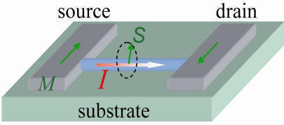
Spin Transport and Spin-Orbit Coupling in Semiconductor and Topological Insulator Nanowires
Conventional electronic devices use the charge of flowing electrons to realize computation and information processing. The concept of incorporating the spin degree of freedom of electrons into the device functionality opened up a new area termed ‘spin-electronics’ (or ‘spintronics’). Much attention of forefront spintronics research has been focused on how to create and control spin polarized current in semiconductors. Recently, researchers have achieved some success in doing so in bulk or thin-films of semiconductors. We are investigating if one can electrically inject, control and detect spin polarized current in high mobility semiconductor nanowires by ferromagnetic contacts. Here, we focus on semiconductors with strong spin-orbit coupling (e.g. InAs, InSb) and topological quantum materials with unique spin properties (e.g. Bi2Se3). We believe that exploiting the spin degree of freedom and spin-orbit coupling enabled control of spin in high quality nanowire materials will open up many new opportunities in studies of mesoscopic physics, nanoelectronic devices and quantum computing.
Nano-Biosensors
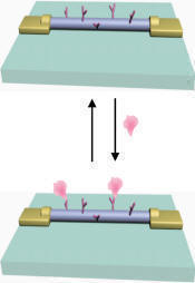
It has been recently demonstrated that nanowire field-effect- transistors can work as sensors to detect extremely low concentration (fMs) of biological molecules in solution. This is intimately related to the small diameter (~10nms) and high quality of semiconductor nanowires. Further development and understanding of such sensors would be essential for the emergence of new technologies in disease diagnostics and drug screening. We are developing chemical and bio-molecule sensors based on nanoelectronic devices (nanowire transistor, nano-capacitors etc). Our focus is placed on understanding the sensing mechanism and biomolecular reaction dynamics at nanosensor surfaces. I also have interest in using nano-electronic devices in biophysics research, single molecule study of biomolecular reactions, to give an example. This research is highly interdisciplinary and can lead to exciting advancements in multiple areas including bio-physics, surface chemistry, and biotechnology.
Nanowire Thermoelectrics for Energy Conversion
Thermoelectric materials can generate electrical power when a thermal gradient is imposed along the sample, providing a means to convert thermal energy into electricity. Thermoelectrics has been studied since the 1960.s but so far has received limited application because of the low efficiency. In recent years, there has been a growing interest in thermoelectric applications of nano-structured materials, in which the electrical and thermal properties (electrical conductivity, thermopower, and thermal conductivity) can be tailored through proper material design. We are experimentally studying nanowires as thermoelectric materials for efficient energy conversion. The expected results will advance our understanding of the effect of low dimensionality on the thermoelectric energy conversion efficiency, and provide guidelines for developing new nanomaterials-based thermoelectrics as an alternative energy source. This project is funded partly by ACS Petroleum Research Fund through grant #48800-DNI10.

Collaborative research with other research groups
We have collaborations with the following research groups:
Prof. Mohan Sankaran, Dept of Chemical Engineering, CWRU (nanomaterial synthesis and devices)
Prof. Clemens Burda, Dept of Chemistry, CWRU (halide perovskite solar cell materials)
Prof. Alp Sehirlioglu, Dept of Material Sciences, CWRU and NASA Glenn Research Center (novel 2D carrier systems at oxide heterostructure interfaces)
Prof. Marie-Helene Berger, Ecole de Mines, Paris (transmission electron microscopy study of oxide hetero-interface)
Prof. Wei Lu, Univ of Michigan (functional devices based on oxide hetero-interface)
Prof. Walter Lambrecht, CWRU Physics (theory of oxides and 2D semiconductor materials)
Prof. Alex Demkov, Dept of Physics, Univ of Texas, Austin (oxide hetero-interfaces)
Prof. John Ekerdt, Dept of Chemical Engineering, Univ of Texas, Austin (oxide hetero-interfaces)
Prof. Loren Pfeiffer, Electrical Engineering, Princeton (strongly correlated 2D carriers in semiconductors)
Prof. Mike Manfra, Electrical Engineering, Purdue (strongly correlated 2D carriers in semiconductors)
Prof. Rui He, University of Northern Iowa (Raman spectroscopy of low dimensional nanostructures)
Prof. Philip Feng, CWRU, EECS (2D semiconductor devices)
Prof. Zhidong Zhang and Prof. Zhenhua Wang, Institute of Metal Research, Chinese Academy of Sciences (topological insulator nanomaterials)
Prof. Fang Cheng Chou and Prof. Yit-Tsong Chen, National TaiWan University (2D materials)
Prof. Qihua Xiong, Nanyang Technology University, Singapore (nanomaterials)
Prof. Hongjun Gao, Institute of Physics, Chinese Academy of Sciences (quantum transport in semiconductor nanowires)
Prof. Iwan Alexander, Dept of Mechanical and Aerospace Engineering, CWRU/Univ of Alabama (nanoscale pressure and flow sensors)
Prof. Alexis R. Abramson, Dept of Mechanical and Aerospace Engineering, CWRU (bismuth nanowires)
Prof. Corey Smith, Dept of Physiology and Biophysics, CWRU (nanobiosensor)
We also work with the National High Magnetic Field Lab on ultra-low temperature studies of 2D electronic systems.
Research Sponsors
We acknowledge the following funding sources for supporting our research.

National Science Foundation
grant # DMR-1607631, “Solid-liquid transition and intermediate state formation in strongly correlated 2D systems” (ongoing)
grant # DMR-1151534,”CAREER Award: Tailoring the Surface State Conduction in Semiconductor and Topological Insulator Nanowires” (ongoing)
grant # DMR-0906415 (completed)

Air Force Office of Scientific Research
grant# FA9550-18-1-0030, “Controlled nanostructures of atomically thin 2D oxides for next generation functional materials” (2018-2021, ongoing)
grant # FA9550-12-1-0441, “Quantitative Identification of Electro-Physical Properties of Hetero-Interfaces at Extreme Environments” (2012-2017, completed)

ACS Petroleum Research Fund
grant #48800-DNI10, “Nanowire thermoelectrics” (completed)
Case Western Reserve University, IAIG pilot grant (completed)